
In chip resistor manufacturing, G2 ink does not provide conductivity, but its core role is to deliver excellent electrical insulation protection, making it critical to product stability. In particular, after laser trimming, if the cut is not properly covered, subsequent plating, high-temperature/high-humidity tests, or other environmental testing may cause resistance drift, reduced adhesion, and other issues.
Therefore, G2 ink should not be viewed only as a surface-protection layer. You must also consider material design, printability, and whether the drying and curing (sintering) conditions are properly matched.
Starting from chip-resistor process requirements, this article summarizes the role definition of G2 ink, key formulation considerations, critical points for process integration, and the likely root causes behind common issues.
Contents
I. What Is Protective Overcoat Ink for Chip Resistors (G2 Ink)?
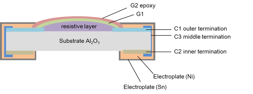
Chip resistors are mainly manufactured by screen printing. Electrodes and the resistive element are first formed on a ceramic substrate, the resistance value is then adjusted by laser trimming, and finally a protective layer and side electrodes are applied to complete the overall structure.
In this process, the role of G2 protective ink is not simply to cover the surface; it is responsible for protecting the fine cuts left after laser trimming, preventing sensitive areas from being exposed during subsequent processes and in end-use environments. If the cut is not properly covered, the chip resistor may experience resistance drift under conditions such as plating, high temperature/high humidity, high voltage, or soldering—ultimately affecting long-term reliability.
Therefore, G2 ink is an important protective layer that affects chip-resistor stability. From a process perspective, it simultaneously serves as an insulating barrier, a protective overcoat, and a contributor to overall product stability.
II. Core Functions of G2 Ink and Key Formulation Considerations
The performance of G2 ink does not come from a single raw material. It depends on how the resin, filler, and solvent are balanced—and how the formulation fits the customer’s process conditions. If you focus on only one material property while ignoring overall formulation design, real process problems are often not resolved.
| Component | Design Focus | Impact on Performance |
|---|---|---|
| Resin system | Thermoset epoxy-based; control crosslink density | Affects heat resistance, insulation, adhesion, chemical resistance, and environmental durability |
| Filler | 1. Adjust screen-print operability 2. Use high-purity filler powders to control film formation and hardness |
1. Print uniformity and pattern stability 2. Influences thickness stability, surface smoothness, and post-cure mechanical strength |
| Solvent | Adjust evaporation rate and boiling point to match printing and drying conditions | Affects print uniformity, film quality, and surface condition after drying |
For the resin system, epoxy resin is widely used in G2 ink mainly because crosslinking design enables a balance of insulation, high-temperature resistance, adhesion to ceramic substrates, and resistance to acids/alkalis, plating solutions, and high-temperature/high-humidity environments.
In addition to adjust operability for the customer, fillers also directly affect film thickness, surface smoothness, and hardness. If filler purity or dispersion is poor, it often degrades printed film quality and may even impact downstream reliability.
As for solvents, they are closely tied to screen-printing behavior and drying performance. If evaporation is too fast, it can cause uneven surfaces, bubbles, or pinholes; if evaporation is too slow, solvent may remain during subsequent heating, leading to tackiness or incomplete curing.
III. Why Can G2 Ink Affect Yield?
Many abnormal issues in chip resistors appear to be caused by the resistive element or process equipment, but in practice they are often related to a mismatch between G2 ink properties and process conditions. This impact becomes even more evident as component sizes continue to shrink and customers demand higher reliability.
| Common symptom | Likely cause | Impact on product |
|---|---|---|
| Resistance drift | Incomplete coverage of the laser cut; insufficient insulation protection | Resistance value deviates from the original design specification |
| overflow / ragged edges | Viscosity too low or insufficient thixotropy | Affects pattern precision and dimensional stability |
| Mesh marks / non-uniform thickness | Thixotropy too high; poor leveling | Local thin spots lead to unstable insulation strength |
| Poor adhesion | Insufficient curing; uneven stress distribution | Peeling or cracking, affecting downstream processes |
| Plating attack | Insufficient chemical resistance or incomplete crosslinking | Leakage, failure, or resistance drift |
The common thread across these issues is that they are usually not caused by a single material defect. Instead, they result from poor alignment among ink formulation, printing conditions, drying rate, and curing condition settings. In other words, whether a G2 ink is suitable should not be judged by one specification number alone—it must be evaluated together with the overall process conditions.
IV. How Should Process Conditions Be Matched with G2 Ink Properties?
Selecting G2 ink cannot be done from the material side alone; it must be assessed against real process conditions. Different mesh counts, target film thicknesses, resistor sizes, and printing speeds all influence the optimal viscosity and thixotropy settings.
1. Screen-printing conditions and viscosity settings
In chip-resistor screen printing, G2 ink is typically used with screens of about 200–400 mesh. In general, a common viscosity setting is around 30,000–50,000 cps, balancing printing stability and film quality.
| Item | Recommended range |
|---|---|
| Mesh count | Approx. 200–400 mesh |
| Viscosity | Approx. 30,000–50,000 cps |
If viscosity is too low, the ink may overflow after printing, causing ragged edges. If viscosity is too high, it can reduce print uniformity and surface smoothness, increasing the risk of downstream defects.
2. Ink selection logic for different chip sizes
Different chip-resistor sizes have different requirements for ink flow and film-thickness control. This is why a single ink grade may not be suitable for every size.
| Size | Recommended ink characteristic | Reason |
|---|---|---|
| 0402 and below | Lower viscosity | Thinner film; improve flow and printing efficiency |
| 0603 and above | Higher thixotropy | Thicker film; avoid spreading and overflow |
For small-size products, lower-viscosity inks are typically needed to maintain stable printing with thinner films. For medium to larger sizes, as film thickness increases, overly high flow can cause overflow, so higher thixotropy is often required to maintain pattern stability.
3. Impact of thixotropy (Ti value) on print quality
Thixotropy is a very important parameter in G2 ink, with especially significant impact on thick films and pattern-stability control.
| Ti value | Typical issue | Impact on product |
|---|---|---|
| Too low | Ink overflow; blurred edges; may flow into gaps | Affects original resistor design and resistance stability |
| Too high | Mesh marks; non-uniform thickness | Insufficient insulation, reduced adhesion, higher risk of peeling or cracking |
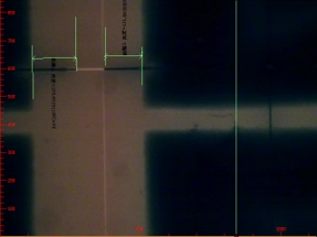
Microscope photo of a case with Ti value too low
When the Ti value is too low, the ink can spread outward after printing and may even enter areas that should not be covered—directly impacting the original product design. Conversely, when the Ti value is too high, obvious mesh marks may remain, creating locally thin regions. This can weaken insulation strength or cause adhesion issues after curing due to stress concentration.
V. Key Controls for Drying and Curing
In addition to printing conditions, drying and curing are also critical steps that determine the final performance of G2 ink. Many practical abnormalities do not originate at the moment of printing, but from improper settings in downstream heating conditions.
1. Drying process control
The purpose of drying is to allow solvent to evaporate appropriately and to build a stable film structure. A commonly recommended condition is about 150–180°C for 10–30 minutes, but actual settings should still be adjusted based on formulation and line speed.
If drying time is too short, solvent may not fully evaporate, which can lead to tackiness during broking to strike or subsequent stacking. If temperature is greatly increased to pursue production capacity, overly fast surface evaporation may cause bubbles, pinholes, and poor surface leveling.
2. Curing and degree of crosslinking completion
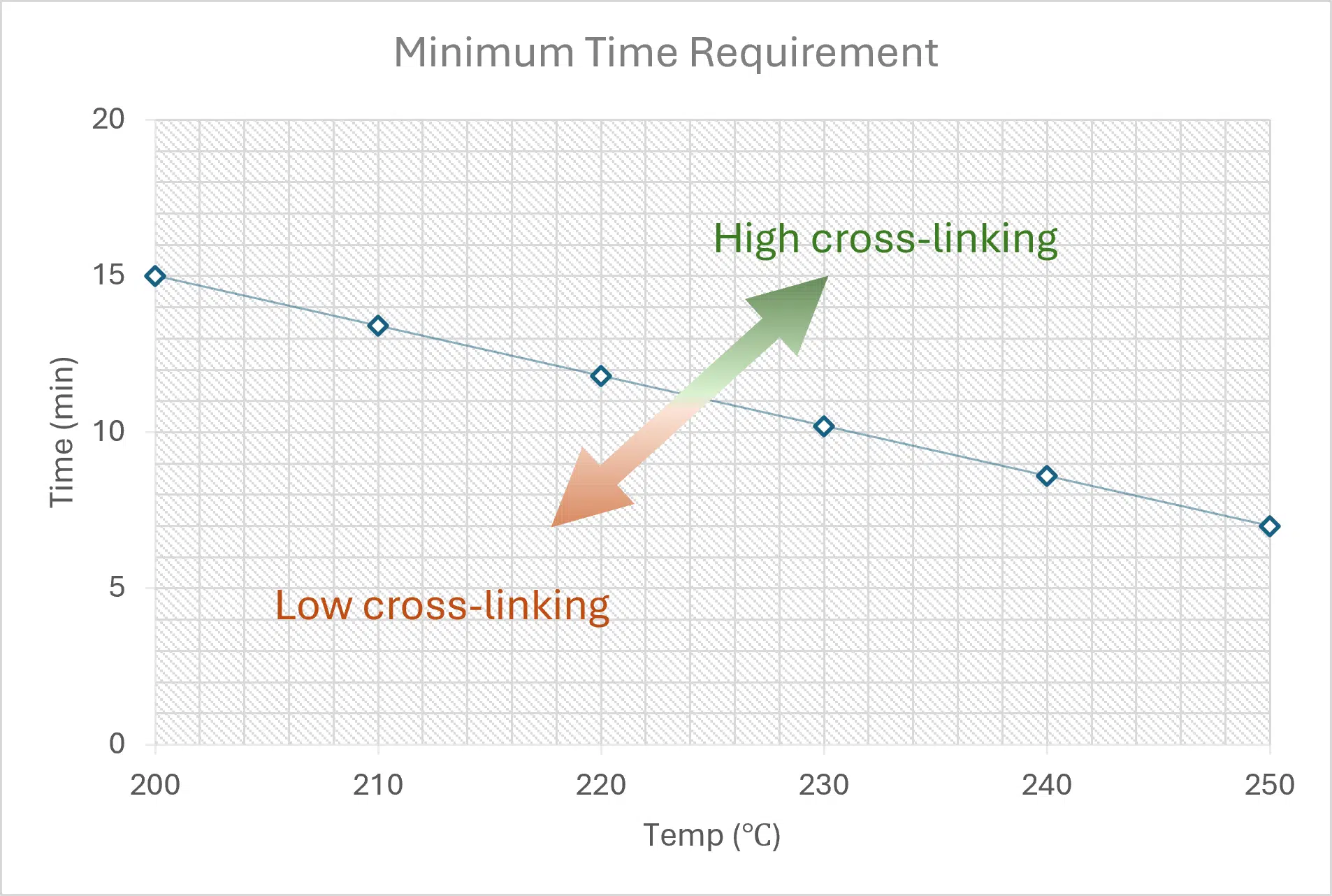
For epoxy resin systems, curing is not merely a heating step—it is the key stage that determines the degree of crosslinking. Generally, only when crosslinking completion reaches above 95% can the material’s intended performance in heat resistance, insulation, adhesion, and environmental durability be more fully realized.
If curing time is insufficient or the temperature setting is too low, common risks include :
- Insufficient hardness, unable to meet standard requirements (above 4H)
- Reduced adhesion to the ceramic substrate or the G1 layer
- Lower chemical resistance and environmental durability
- Increased risk of plating-solution attack
- Higher probability of resistance drift or failure
In other words, many issues that seem to be caused by the material itself are in fact the result of incomplete curing. If drying and curing conditions are overlooked, even a well-designed formulation may fail to deliver its intended performance.
Recommended G2 ink curing conditions can be evaluated using the degree-of-crosslinking curve shown below: when temperature and time are above the minimum requirement line, crosslinking completion is higher; if below this region, insufficient curing may occur.
VI. When Can a Single G2 Ink Grade Not Meet All Product Requirements?
In actual production, different chip-resistor sizes do not have the same requirements for G2 ink. Small-size products typically need lower viscosity to maintain flow; medium to large sizes place greater emphasis on thixotropy control to avoid spreading and overflow. Therefore, when a single line covers multiple sizes, film-thickness targets, or reliability requirements, one ink specification may not cover everything.
In practice, if the applicable viscosity ranges of different products still overlap sufficiently, a single ink may still be feasible. However, if the overlap is not enough—especially when it is less than about 8,000 cps—two or more ink grades are usually needed to maintain printing stability and yield.
VII. Epolab Chemical G2 Ink Application Solutions
To meet application needs for chip-resistor protective overcoat inks, Epolab Chemical provides epoxy-resin-based G2 ink solutions that can be adjusted for different process conditions, chip sizes, and reliability requirements.
Rather than just looking at the product model it's more important to first clarify what kind of problem the current manufacturing process is trying to solve—printing stability, humidity resistance, resistance change rate, or long-term stability in high-reliability environments.
1. Standard process introduction: EI-347 series
If your current focus is general industrial applications and standard process introduction, you can start by evaluating the EI-347 series. This series provides good humidity resistance, a low resistance change rate, and excellent storage stability, with recommended storage at 0–10°C. Epolab Chemical has dozens of customers using this series for more than 15 years, making it a solid baseline option for most standard processes.
In addition, the EI-347 series can be further customized to customer needs by adjusting viscosity, thixotropy, and special colors, helping different production lines achieve better printing stability.
2. High humidity resistance & high reliability needs: EI-547 series
If the product must meet more stringent humidity resistance, high-reliability, or automotive-grade requirements, you can further evaluate the EI-547 series. This series uses a specially designed hydrophobic resin structure and offers better humidity resistance than the EI-347 series.
Based on laboratory testing, after printing on a ceramic substrate and performing a water-immersion test, the EI-347 series shows a water absorption of about 1.2%, while the EI-547 series is about 0.83%, giving it an advantage in humidity resistance. In addition, customer records indicate the EI-547 series can control resistance change within an acceptance criterion of ±0.1%, and it has been successfully introduced into high-end and automotive products.
| Series | Key features | Recommended applications |
|---|---|---|
| EI-347 series | Good humidity resistance, low resistance change, excellent storage stability (0–10°C) | General industrial applications; standard process introduction |
| EI-547 series | Special hydrophobic structure design; water absorption ~0.83%; higher humidity resistance | High-end applications; automotive products; harsh-environment requirements |
If you are deciding whether to use a standard grade or a high-humidity-resistance solution for your process, it is recommended to provide chip size, required film thickness, screen-printing conditions, and reliability requirements. Evaluating materials together with process conditions helps identify the most suitable G2 ink direction.
VIII. Frequently Asked Questions (Q&A)
A: Not necessarily. Resistance drift may result from insufficient coverage of the post-trim laser cut, improper drying or curing conditions, or poor overall process matching. In practice, you cannot evaluate the ink alone; both material and process must be checked together.
A: If the abnormality mainly shows up as overflow, ragged edges, mesh marks, or local non-uniform thickness, check viscosity and Ti settings first. If the abnormality appears as reduced adhesion, insufficient hardness, worse chemical resistance, or post-plating failures, further check whether drying and curing conditions have led to incomplete curing.
A: Because different chip sizes require different film thickness, flow behavior, and printing stability. Small sizes usually need lower viscosity, while medium to large sizes rely more on thixotropy control—so one formulation may not cover everything.
A: Evaluate using a combination of hardness, adhesion, chemical resistance, and environmental tests. If hardness cannot reach above 4H, adhesion declines, or abnormalities occur after plating and high-temperature/high-humidity testing, you should review the crosslinking completion level and curing conditions.
IX. Stability Comes from Matching Materials and Process
Protective overcoat ink for chip resistors (G2 ink) is not only a protective material in the process—it is also a key factor that influences stability, yield, and reliability. From formulation design of resin, filler, and solvent to process controls such as screen printing, drying, and curing, every step affects final performance.
For engineers and purchasing teams, selecting G2 ink should not rely on a single specification or product model. Instead, it should be assessed against chip size, film-thickness requirements, process conditions, and environmental demands. When materials and process truly match, abnormal risks can be reduced and overall process stability can be improved.
If you are evaluating which protective overcoat ink to use for chip resistors, you can first organize your current size specifications, screen-printing conditions, and reliability requirements. This will help focus material evaluation and make it easier to identify a suitable solution.